


0 reviews
Be the first to review this item!


| Derate Above 25°C | 5.0 mW/°C | |
| Max. drain to gate voltage | 35 V | |
| Max. forward gate current | 50 mA | |
| Max. gate to source voltage | -35 V | |
| Operating and Storage Junction Temperature Range | -55 to 150 °C | |
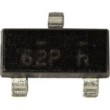
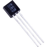
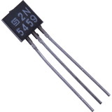
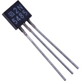
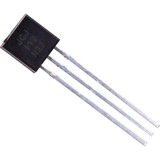
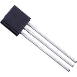
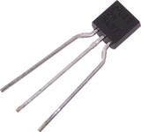
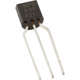
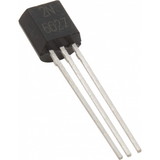
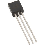
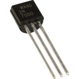
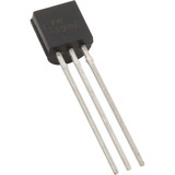
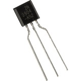
| Package | TO-92 | |
| Thermal Resistance, Junction?to?Ambient | 200 °C/W | |
| Thermal Resistance, Junction?to?Case | 125 °C/W | |
| Total Device Dissipation | 625 mW |
| Packaging Dimensions | 0.752 in. × 0.187 in. × 0.143 in. | |
| Weight (Packaging) | 0.001 lbs. |
 Attention CA Residents: Prop 65 Warning
WARNING:
This product can expose you to chemicals which are known to the State of California to cause cancer, birth defects, or other reproductive harm. For more information, go to www.p65warnings.ca.gov.