


0 reviews
Be the first to review this item!

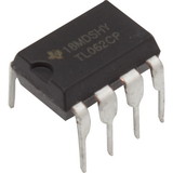
| Amplifier-to-Amplifier Coupling | -120dB | |
| IOS Drift | 10pA/°C | |
| Junction-to-Ambient Thermal Resistance | 88°C/W | |
| Max. Supply Current | 3mA | |
| Max Differential Input Voltage | 32V | |
| Max Input Bias Current (IIN(+) or IIN(?)) | 500nA | |
| Max Input Bias Current (IIN(+) or IIN(?), VCM = 0V, TA = 25°C) | 250nA | |
| Max Input Common-Mode Voltage Range (V+ = 30V) | V+ - 2V | |
| Max Input Common-Mode Voltage Range (V+ = 30V, TA = 25°C) | V+ - 1.5V | |
| Max Input Current (VIN < -0.3V) | 50mA | |
| Max Input Offset Current (IIN(+) or IIN(?), VCM = 0V) | 150nA | |
| Max Input Offset Current (IIN(+) or IIN(?), VCM = 0V, TA = 25°C) | 50nA | |
| Max Input Offset Voltage (TA = 25°C) | 7mV | |
| Max Input Offset Voltage (VO ? 1.4V, RS = 0Ω with V+ from 5V to 30V; and over the full input common-mode range (0V to V+ ? 1.5V)) | 9mV | |
| Max Input Voltage | 32V | |
| Max Lead Temperature (Soldering, 10 Seconds) | 260°C | |
| Max Operating Input Voltage on Input pins | V+ | |
| Max Output Short-Circuit to GND (One Amplifier) | Continuous | |
| Max Power Dissipation | 1130mW | |
| Max Short Circuit to Ground | 60mA | |
| Max Soldering (10 Seconds) | 260°C | |
| Max Supply Voltage (V+ - V-) | 32V | |
| Min Common-Mode Rejection Ratio | 65dB | |
| Min Input Common-Mode Voltage Range (V+ = 30V) | 0V | |
| Min Input Common-Mode Voltage Range (V+ = 30V, TA = 25°C) | 0V | |
| Min Input Voltage | -.3V | |
| Min Large Signal Voltage Gain (V+ = 15V (VOSwing = 1V to 11V), RL ≥ 2kΩ) | 15V/mV | |
| Min Large Signal Voltage Gain (V+ = 15V, RL ≥ 2k?, (VO = 1V to 11V), TA = 25°C) | 25V/mV | |
| Min Operating Input Voltage on Input pins | 0V | |
| Min Power Supply Rejection Ratio | 65dB | |
| Min Sink Output Current | 5mA | |
| Min Sink Output Current (TA = 25°C) | 20mA | |
| Min Source Output Current | 10mA | |
| Min Source Output Current (TA = 25°C) | 20mA | |
| Min Supply Voltage (V+ - V-) | 3V | |
| Operating Junction Temperature | -0°C to 70°C | |
| Storage Temperature Range | -65°C to +150°C | |
| Typical Common-Mode Rejection Ratio | 85dB | |
| Typical Input Bias Current (IIN(+) or IIN(?)) | 40nA | |
| Typical Input Bias Current (IIN(+) or IIN(?) , VCM = 0V, TA = 25°C) | 45nA | |
| Typical Input Offset Current (IIN(+) or IIN(?), VCM = 0V, TA = 25°C) | 5nA | |
| Typical Input Offset Voltage (TA = 25°C) | 2mV | |
| Typical Large Signal Voltage Gain | 100V/mV | |
| Typical Power Supply Rejection Ratio | 100dB | |
| Typical Short Circuit to Ground | 40mA | |
| Typical Sink Output Current | 8mA | |
| Typical Sink Output Current (TA = 25°C) | 10mA | |
| Typical Source Output Current | 20mA | |
| Typical Source Output Current (TA = 25°C) | 40mA | |
| Typical Supply Current | 1.5mA | |
| VOS Drift | 7µV/°C |
| Packaging Dimensions | 0.758 in. × 0.325 in. × 0.285 in. | |
| Weight (Packaging) | 0.002 lbs. |
| Specification Sheet | All Models |
 Attention CA Residents: Prop 65 Warning
WARNING:
This product can expose you to chemicals which are known to the State of California to cause cancer, birth defects, or other reproductive harm. For more information, go to www.p65warnings.ca.gov.