

0 reviews
Be the first to review this item!

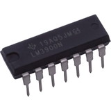
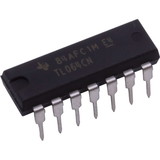
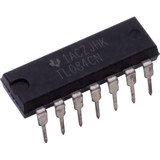
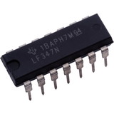
| CMRR - Common Mode Rejection Ratio | 80 dB: | |
| GBP - Gain Bandwidth Product | 2.2 kHz: | |
| Ib - Input Bias Current | 0.6 pA: | |
| Maximum Operating Temperature | + 125 C: | |
| Minimum Operating Temperature | - 55 C: | |
| Number of Channels | 4 Channel: | |
| Operating Supply Current | 2.7 mA: | |
| Operating Supply Voltage | 3 V to 16 V: | |
| Output Current per Channel | 30 mA: | |
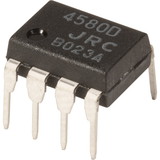
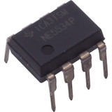
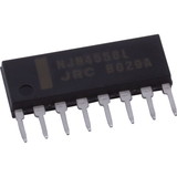
| Package | PDIP-14: | |
| Pd - Power Dissipation | 1575 mW | |
| SR - Slew Rate | 3.6 V/us: | |
| Supply Voltage - Max | 16 V: | |
| Supply Voltage - Min | 3 V: | |
| Voltage Gain dB | 87.23 dB | |
| Vos - Input Offset Voltage | 1.1 mV: | |
| en - Input Voltage Noise Density | 25 nV/sqrt Hz: |
| Packaging Dimensions | 0.712 in. × 0.361 in. × 0.28 in. | |
| Weight (Packaging) | 0.002 lbs. |
| Datasheet | All Models |
 Attention CA Residents: Prop 65 Warning
WARNING:
This product can expose you to chemicals which are known to the State of California to cause cancer, birth defects, or other reproductive harm. For more information, go to www.p65warnings.ca.gov.