


0 reviews
Be the first to review this item!


| Estimated FLASH endurance (Erase/Write cycles) | 10,000 | |
| MEx. DC operating voltage | 3.6 VDC | |
| Max. Clock range in to pin 31 | 12.3 MHz | |
| Max. Input high voltage to SWO - SW4, ENABLE and TAP | VDD | |
| Max. Input low voltage to SWO - SW4, ENABLE and TAP | 0.2* VDD | |
| Max. Internal pull-up equiv resistance | 50 K? | |
| Max. Output low voltage to USER0, USER1 and OFLO | 0.4 VDC | |
| Max. POT0 - POT5 source impedance | 10 K? | |
| Max. Sample rate range as master | 48.046 KHz | |
| Max. Sample rate range as slave | 96 KHz | |
| Max current sink/source through USER0, USER1 or OFLO | 10 mA | |
| Min. Clock range in to pin 31 | 10 MHz | |
| Min. DC operating voltage | 3.0 VDC | |
| Min. Input high voltage to SWO - SW4, ENABLE and TAP | 0.8* VDD | |
| Min. Input low voltage to SWO - SW4, ENABLE and TAP | GND | |
| Min. Internal pull-up equiv resistance | 5 K? | |
| Min. Output low voltage to USER0, USER1 and OFLO | 0 VDC | |
| Min. Sample rate range as master | 9.766 KHz | |
| Min. Sample rate range as slave | 0 KHz | |
| Operating temperature range | -30°C through +80°C | |
| Output high voltage to USER0, USER1 and OFLO | VDD | |
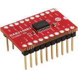
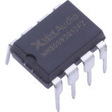
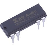
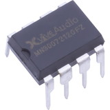
| Package | 64-pin TQFP | |
| Storage temperature range | -50°C through +140°C | |
| Typ. Clock range in to pin 31 | 12.288 MHz | |
| Typ. DC operating current | 110 mA | |
| Typ. DC operating voltage | 3.3 VDC | |
| Typ. Sample rate range as master | 48 KHz |
| Packaging Dimensions | 0.942 in. × 0.662 in. × 0.067 in. | |
| Weight (Packaging) | 0.001 lbs. |
 Attention CA Residents: Prop 65 Warning
WARNING:
This product can expose you to chemicals which are known to the State of California to cause cancer, birth defects, or other reproductive harm. For more information, go to www.p65warnings.ca.gov.